
NEWS
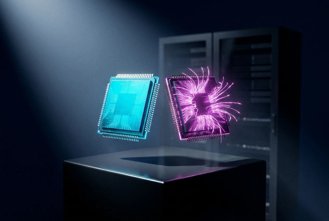
Google Splits TPU 8 Into Two Chips for the Agent Era

Google split its eighth-generation Tensor Processing Unit into two distinct chips this week, an architectural pivot driven by a single fact: training and inference now want physically incompatible hardware. The TPU 8t and TPU 8i, unveiled April 22, 2026 at Google Cloud Next in Las Vegas, are the first generation Google has divided by workload.
Google introduced the chips at Cloud Next 2026 on April 22, splitting its custom accelerator into a training part with 9,600-chip pods delivering 121 ExaFlops, and an inference part with 288 GB of memory built for reasoning agents. Both reach general availability through Google Cloud later in 2026, with Anthropic and Citadel Securities named as early adopters.
The reveal lands in the middle of a multi-gigawatt hardware race. Anthropic, the maker of Claude, has booked 3.5 gigawatts of TPU capacity beginning in 2027, in a deal it confirmed earlier this month with Google and Broadcom.
Why Google Split One Chip Into Two
For seven generations, every TPU was a single design that handled training and serving on the same silicon. That stopped working when reasoning models arrived.
Training rewards huge scale-up bandwidth and tolerates latency, since gradient updates batch across thousands of chips. Inference for agentic workloads is the opposite problem. Each token leaves a chip waiting on a previous calculation, and a single slow link in a swarm of agents magnifies into idle silicon.
“At a time when general-purpose CPUs are really only improving performance 5% a year, you have to specialize if you’re going to go after brand new workloads,” said Amin Vahdat, Google’s SVP and chief technologist for AI and infrastructure, at the keynote. The split is Google’s bet that the agentic era will not be won by a balanced chip.
Inside TPU 8t: A 9,600-Chip Pod Aimed at Frontier Training
TPU 8t is the training half. A single superpod scales to 9,600 chips and pools two petabytes of high-bandwidth memory, delivering 121 ExaFlops of FP4 compute, nearly triple the per-pod throughput of last year’s Ironwood TPU, according to Google’s eighth-generation TPU announcement.
The Virgo Fabric and the Million-Chip Cluster
Pods do not stop at 9,600 chips. Google’s new Virgo network fabric stitches up to 134,000 chips into a single non-blocking cluster, and pushes near-linear scaling out to one million chips across data centers using JAX and the company’s Pathways software.
The fabric delivers roughly 47 petabits per second of bisection bandwidth, four times more than the previous generation, per Google’s technical deep dive on TPU 8t and 8i.
Why “Goodput” Matters More Than FLOPs
Google says TPU 8t targets over 97% goodput, the share of cluster time spent on useful compute rather than recovery from failures. Optical Circuit Switching reroutes around dead links without restarting the job. Real-time telemetry across tens of thousands of chips spots faults before they cascade.
The math is brutal at frontier scale. A 1% drop in goodput on a 9,600-chip pod translates to days of lost training per quarter.
Inside TPU 8i: Cutting Network Hops From 16 to 7
TPU 8i is the inference chip, and its biggest change is not the silicon. It is the way Google wires the silicon together.
The old 3D torus topology was tuned for neighbor-to-neighbor traffic, the pattern of training. Reasoning models talk all-to-all, especially in Mixture-of-Experts routing where any expert may need any token. Boardfly, the new topology, drops the maximum chip-to-chip path in a 1,024-chip pod from 16 hops on a 3D torus to 7 hops, a 56% cut in network diameter.
Each four-chip tray forms a building block. Eight boards form a group connected by copper. Optical Circuit Switches link 36 groups into a pod. The result is dragonfly-style flattening that prefers global reach over local density.
Breaking the Memory Wall
TPU 8i pairs 288 GB of high-bandwidth memory with 384 MB of on-chip SRAM, three times the SRAM of its predecessor. The added on-chip memory is sized to hold the entire KV cache of a production-scale reasoning model on silicon, eliminating round trips to HBM during decoding.
An on-chip Collectives Acceleration Engine, or CAE, handles the reduction and synchronization steps that dominate auto-regressive decoding. Google measured a 5x cut in on-chip collective latency. The chip claims 80% better performance per dollar over Ironwood.
How TPU 8t and TPU 8i Compare
| Spec | TPU 8t (Training) | TPU 8i (Inference) |
|---|---|---|
| Network topology | 3D torus plus Virgo fabric | Boardfly |
| Peak FP4 per chip | 12.6 PFLOPs | 10.1 PFLOPs |
| HBM capacity | 216 GB | 288 GB |
| HBM bandwidth | 6,528 GB/s | 8,601 GB/s |
| On-chip SRAM | 128 MB | 384 MB |
| Max pod scale | 9,600 chips | 1,152 chips |
| CPU host | Arm Axion | Arm Axion |
The Anchor Customers Behind the Launch
Two names dominate the customer slide. Anthropic, which earlier this month released Claude Opus 4.7, has committed to up to one million TPU chips and 3.5 gigawatts of compute beginning in 2027. Citadel Securities, the high-frequency market maker, runs quantitative research on TPUs and was the only outside firm Google quoted on stage.
Citadel previously disclosed it can spin up more than one million cores concurrently on Google Cloud for parallel research jobs. The TPU 8 announcement positions reasoning workloads, not just training, as the next bottleneck the firm is buying against.
“It’s not just 9,600 chips that are working on a problem. In many cases, it’s tens of thousands, and, dare I say, more, that are all coordinating together at literally nanosecond scale,” Vahdat said during the keynote.
Power Is the Real Ceiling
Google says TPU 8t and TPU 8i deliver up to 2x performance per watt over Ironwood. That number matters because power, not chip supply, is now the binding constraint on data center growth.
The chips ride on Google’s fourth-generation liquid cooling distribution unit and run on the company’s Arm-based Axion CPU host, the first time Google has paired its own CPU and TPU in the same rack. Arm confirmed the Neoverse V2 design partnership last year. By owning host, accelerator, network, and cooling, Google is making a familiar argument: vertical integration beats the open ecosystem on watts.
Google says its data centers now deliver six times more compute per unit of electricity than five years ago.
What This Means for Nvidia
The split is not aimed only at Nvidia, but the comparison is unavoidable. Nvidia’s GB300 NVL72 rack delivers about 1.1 ExaFlops of FP4 compute. A TPU 8t pod, at 121 ExaFlops, equals more than a hundred GB300 racks of throughput, though the comparison flatters Google because rack and pod are not the same unit.
The harder fight is software. CUDA still defines the AI training workflow for most labs. Google’s counter is open framework support: native PyTorch, vLLM, SGLang, JAX, and bare-metal access for customers who want the host without the hypervisor. The same playbook helped Meta’s Muse Spark superintelligence push attract a similar mix of cloud-native AI shops over the past quarter.
Frequently Asked Questions
When will TPU 8t and TPU 8i Be Available?
Both chips reach general availability through Google Cloud later in 2026. Google began taking interest registrations on April 22, 2026, the day of the announcement.
What Is the Difference Between TPU 8t and TPU 8i?
TPU 8t is built for training, with more compute throughput, larger pods of 9,600 chips, and heavy interchip bandwidth. TPU 8i is built for inference and reasoning agents, with more on-chip SRAM at 384 MB, more HBM at 288 GB, and the new Boardfly topology that cuts network latency.
Who Is Using Google’s TPU 8 Chips?
Anthropic is the largest disclosed customer, with a deal covering up to one million chips and 3.5 gigawatts of capacity from 2027. Citadel Securities was named on stage at Cloud Next 2026 as an existing TPU user planning to adopt the new generation. Google’s Gemini family of models also runs on TPUs.
How Does TPU 8 Compare to Nvidia’s GB300?
A single TPU 8t superpod delivers 121 ExaFlops of FP4 compute across 9,600 chips, while Nvidia’s GB300 NVL72 rack delivers about 1.1 ExaFlops across 72 GPUs. Per-chip, Nvidia and Google are closer than the pod numbers suggest, but Google argues its scale-out fabric and per-watt efficiency win on total cost of ownership.
What Is Boardfly, and Why Does It Matter?
Boardfly is Google’s new network topology for TPU 8i. It replaces the 3D torus used in earlier TPUs with a high-radix design that drops the maximum chip-to-chip path in a 1,024-chip pod from 16 hops to 7. That cut directly reduces tail latency for reasoning agents, which talk to many chips at once rather than just neighbors.
The Pod That Has to Hold the Internet’s Agents
Google’s pitch is that the next decade of AI will not be one giant model on one giant cluster. It will be swarms of agents calling each other in long loops, judged on tail latency rather than peak throughput. TPU 8t and TPU 8i are an architectural answer to that bet, and the price of being wrong is now measured in gigawatts. The next test arrives when Anthropic’s first 3.5 gigawatt block of TPU 8 capacity lights up in 2027.

-
 TECH1 year ago
Where Garmin Watches are Made and How They are Assembled
-

 AUTO2 months ago
Tesla’s Roadster Is ‘a Few Weeks Away,’ Says Its Chief Designer
-
 NEWS10 years ago
Samsung Releases Galaxy Note7 TV Ad as Reddit AMA Leaks Specs
-
 NEWS10 years ago
Android 7.0 Nougat Rolls Out To Nexus Devices With New Emoji, Features
-
 FINANCE9 years ago
Cardano Price Surges as ADA Enters the Crypto Top Ten List
-
 NEWS10 years ago
Pre-Order the First Camera Made for Facebook Live Streaming Video
-
 FINANCE1 year ago
Binance Suspends Trading and Withdrawals for a System Upgrade
-
 FINANCE9 years ago
RChain Price Jumps Nearly 150% to a New All-Time High of $2.03