NEWS
Samsung Foundry Deepens EDA Alliances as Customers Sign On
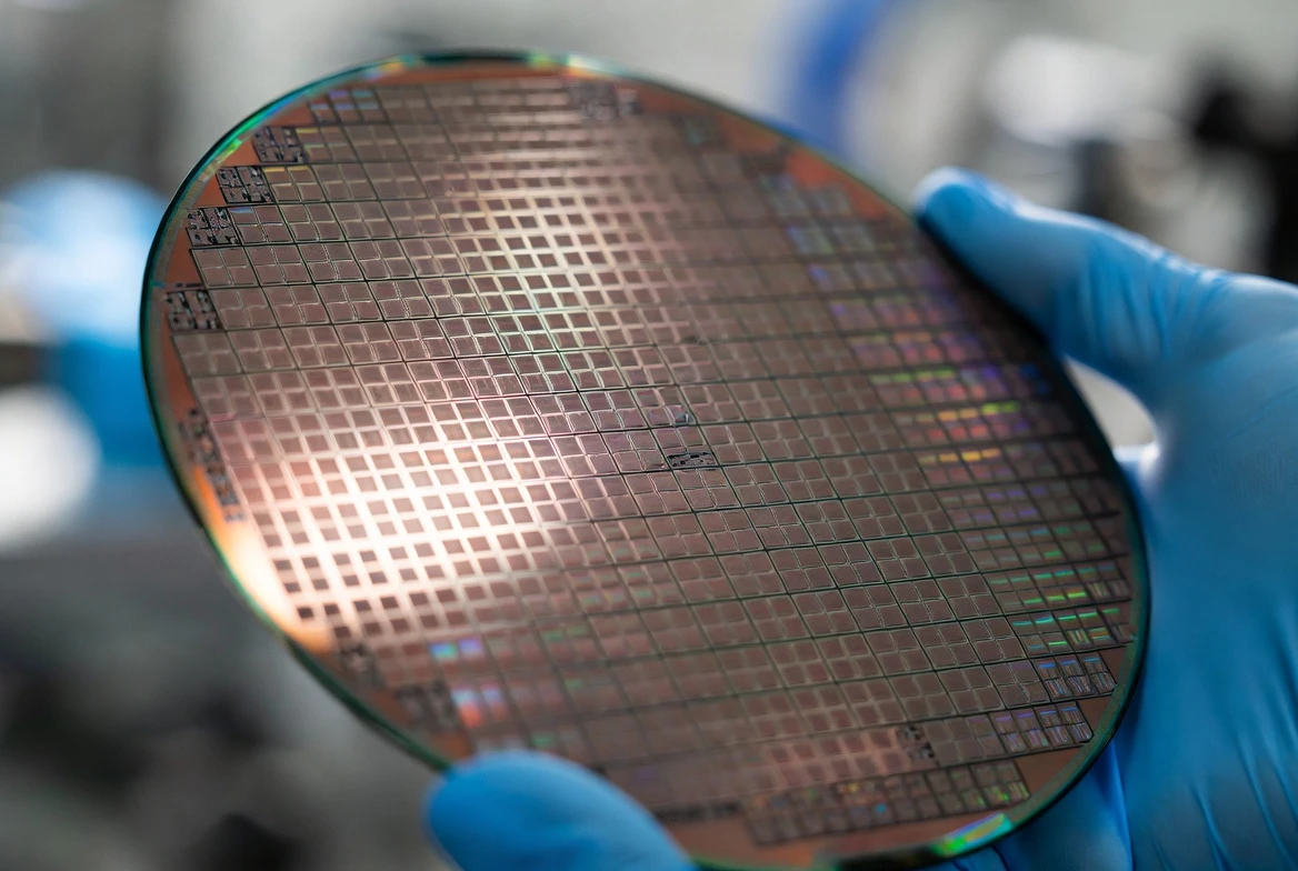
Samsung Foundry deepened its multi-year alliances with chip-design software makers Synopsys and Cadence at SAFE Forum 2026 on May 28, unveiling AI-assisted electronic design automation (EDA, the software used to lay out and verify chips), production-ready second-generation 2nm flows, and hybrid copper bonding for stacked dies. The stated goal is to cut design risk and shorten development for customers building artificial intelligence and high-performance computing (HPC) silicon.
Buried in the same two announcements were three names that matter more than any tool: NVIDIA, Tesla and Ambarella, each now validating designs on Samsung’s newest 2nm process. For a foundry sitting at roughly a tenth of TSMC’s market share, that roster, not the software, is the comeback signal worth tracking.
What Samsung Put on the SAFE Forum Stage
The two press releases read like a tools catalog, but the substance is a tighter handoff between chip designers and Samsung’s fabs on its leading-edge nodes. Both vendors certified flows on second- and third-generation 2nm-class processes, and both extended into 3D-IC (three-dimensional integrated circuits, where dies are stacked vertically rather than placed side by side) using Samsung’s hybrid copper bonding (HCB, a bonding method that joins stacked chips with copper-to-copper contacts for denser, faster links).
Synopsys: Test Cuts and 3D Signoff
Synopsys said its certified flows deliver up to 20% reduction in test patterns and cycles while holding fault coverage, plus up to 2.7% frequency improvement within a 5% leakage budget. Its 3DIC Compiler is being validated on an HCB 3D test chip, replacing manual, margin-heavy design with automated signoff across compute, memory and packaging.
The company also expanded certified interface intellectual property (IP, pre-built design blocks customers license rather than build), covering UCIe (Universal Chiplet Interconnect Express), PCIe 7.0, 112G and 224G links, LPDDR6 and USB4. You can read the SAFE Forum 2026 design enablement details in the company’s own Synopsys foundry collaboration release.
Cadence: Glitch Power and 3D Cube-H
Cadence focused on second-generation 2nm features, including glitch-power optimization folded into its Innovus place-and-route flow and its Cerebrus chip explorer. For stacking, it enabled Samsung’s 3D Cube-H design with a full planning-to-signoff path for HCB.
Notably, Cadence said that flow supports NVIDIA’s NVLink-C2C interconnect and PCIe 5.0, the kind of plumbing data-center accelerators depend on. That detail is where the tools story quietly becomes a customer story.
| Vendor | Headline tools | What it enables on Samsung 2nm and 3D-IC |
|---|---|---|
| Synopsys | 3DIC Compiler, Fusion Compiler, TestMAX, PrimeShield, Totem-SC | Up to 20% test-pattern cuts; up to 2.7% frequency gain; certified UCIe, PCIe 7.0 and LPDDR6 IP; HCB 3D test-chip signoff |
| Cadence | Innovus, Cerebrus, Integrity 3D-IC, Voltus, Pegasus, Virtuoso | Glitch-power optimization for second-gen 2nm; 3D Cube-H with HCB; NVLink-C2C and PCIe 5.0 design support |
The Customer Names in the Fine Print
EDA upgrades arrive every quarter. What made these two announcements different was who agreed to be quoted inside them. Tool certifications are table stakes; named customers vouching for a process node on the record are not.
Three customer endorsements stood out, each tied to a different slice of the AI buildout:
- NVIDIA – Timothy Costa, vice president of computational engineering, said the company is using Cadence’s GPU-accelerated flows on Samsung’s second-generation 2nm to optimize next-generation AI architectures.
- Tesla – the automaker’s reported $16.5 billion chip deal routes its AI5 and AI6 processors to Samsung’s Taylor, Texas fab on a 2nm process, anchoring the foundry’s external order book.
- Ambarella – chief operating officer Chan Lee said a signoff-ready, co-optimized IP and tools package let his teams move forward with less risk on advanced designs.
None of this guarantees volume. But a year ago the open question was whether anyone outside Samsung’s own product groups would trust its leading-edge lines. Having NVIDIA, Tesla and Ambarella attach their names to the enablement flows answers part of that question in public.
The Yield Gap That Still Decides Everything
Design tools shorten the path from idea to tape-out. They do not, by themselves, lift the percentage of working chips that come off a wafer. That number, yield, is where Samsung’s comeback still meets resistance, and it is the variable the SAFE Forum announcements cannot fix.
Samsung’s foundry business has spent two years trying to convince customers its advanced nodes can match the consistency they get elsewhere. The EDA alliances reduce design integration risk; they leave manufacturing risk untouched.
Where Samsung’s Second-Gen 2nm Stands
Reporting on Samsung’s 2nm yields has been a moving target. TrendForce flagged figures in the 55% to 60% band late last year, and a follow-up put them around the mid-50% range in April, below the rough 60% threshold many treat as the floor for stable mass production.
More recent industry chatter around the SF2P process points higher, near 70%, helped by the Tesla orders restoring confidence. The spread itself tells the story: outside observers still cannot agree on where Samsung’s yield actually lands, which is its own kind of risk. The detail sits in TrendForce’s reading of Samsung’s reported 2nm yield range.
The Lead TSMC Still Holds
The scoreboard remains lopsided. TrendForce put TSMC at a 70.2% foundry revenue share in the second quarter of last year, with Samsung second at 7.3%, and TSMC’s 2nm yields reportedly running higher and steadier.
Here is the cluster of figures that frames the gap:
- 7.3% Samsung’s reported second-quarter foundry revenue share, against TSMC’s 70.2%
- mid-50% the reported second-generation 2nm yield band as of April
- 80%+ Samsung Foundry utilization in the first quarter, its highest in over a year
Why Foundries and Tool Makers Keep Merging Roadmaps
There is a structural reason these alliances keep getting tighter, and it predates this year’s event. As AI accelerators push past the limits of a single die, chipmakers stack memory and logic together, which multiplies the physics a designer has to check before committing to silicon.
Heat, power delivery and signal timing now have to be co-optimized across multiple stacked dies at once. No design team wants to discover a thermal or power-integrity problem after a multimillion-dollar mask set is cut. That is why Synopsys and Cadence are embedding HCB and 3D signoff directly into their flows rather than bolting it on later.
The same vertical-stacking pressure is reshaping the memory Samsung sells alongside its foundry services, as our coverage of Samsung’s HBM4E push in the AI memory race lays out. Foundry, packaging and high-bandwidth memory are increasingly one engineering problem, not three.
What the Investor Case Now Rests On
For shareholders watching KOSE:A005930, the alliances add a data point, not a thesis. Samsung Electronics spans memory, logic and consumer electronics, and the stock has run hard into this news. Simply Wall St noted shares at ₩317,000, up about 43.8% over 30 days and trading below both its analyst target of ₩385,641 and its estimated fair value.
The bull case is straightforward: customer validation plus rising utilization plus a 2027 path to foundry profitability once the Taylor fab ramps. The risk sits on the same page. Execution on yield, packaging and delivery timelines against TSMC is the swing factor, and the yield uncertainty laid out in TrendForce’s earlier assessment of Samsung’s 2nm GAA progress has not gone away.
Samsung’s wider chip business is also leaning on adjacent wins to carry the story while foundry stabilizes, including its lead in automotive memory as China reshapes that market. The foundry pieces are lining up; whether they convert into disclosed design wins and clean yield numbers is what the next several quarters will settle.
Frequently Asked Questions
What did Samsung Foundry announce at SAFE Forum 2026?
Samsung extended multi-year alliances with Synopsys and Cadence on May 28, certifying AI-assisted design flows on second- and third-generation 2nm processes, adding 3D-IC signoff for hybrid copper bonding, and expanding interface IP such as UCIe, PCIe 7.0 and LPDDR6 for AI and high-performance computing customers.
Which customers are using Samsung’s second-generation 2nm process?
NVIDIA, Tesla and Ambarella were named in the announcements. NVIDIA cited Cadence flows on Samsung 2nm for AI architectures, Tesla is routing its AI5 and AI6 chips to Samsung’s Texas fab under a reported $16.5 billion deal, and Ambarella’s COO endorsed the co-optimized tools and IP package.
How does Samsung’s 2nm yield compare with TSMC’s?
Reports vary. TrendForce put Samsung’s 2nm yields in the mid-50% range as of April, below the roughly 60% threshold for stable mass production, while newer chatter on the SF2P process points near 70%. TSMC’s 2nm yields are widely reported as higher and more consistent.
What is hybrid copper bonding and why does it matter?
Hybrid copper bonding joins stacked chips with direct copper-to-copper contacts instead of solder bumps, enabling denser, faster connections between dies. It is central to 3D-IC designs for AI accelerators, which is why both Synopsys and Cadence built HCB signoff into their Samsung flows.
Is Samsung Electronics stock undervalued in 2026?
Simply Wall St viewed the stock as undervalued, with shares around ₩317,000 trading below the ₩385,641 analyst target and its estimated fair value, after a roughly 43.8% gain over 30 days. That view depends on execution risk in yield and timelines, so investors should treat it as one input, not advice.
Disclaimer: This article is for informational purposes only and is not financial advice. It covers equities and semiconductor-sector investing, which carry execution, market and valuation risk. Consult a qualified financial professional before making investment decisions. Figures, including share prices and analyst estimates, are accurate as of publication and may change.
-
 NEWS10 years ago
Samsung Releases Galaxy Note7 TV Ad as Reddit AMA Leaks Specs
-
 NEWS10 years ago
Android 7.0 Nougat Rolls Out To Nexus Devices With New Emoji, Features
-
 FINANCE8 years ago
Cardano Price Surges as ADA Enters the Crypto Top Ten List
-
 NEWS10 years ago
Pre-Order the First Camera Made for Facebook Live Streaming Video
-
 FINANCE8 years ago
RChain Price Jumps Nearly 150% to a New All-Time High of $2.03
-
 FINANCE10 months ago
Binance Suspends Trading and Withdrawals for a System Upgrade
-
 NEWS10 years ago
Google Play App Icons Get Fresh New Look: See the Latest Design Update
-
 NEWS10 years ago
Google Doodle Go Bananas Fruit Games Live On Mobile For Two Weeks