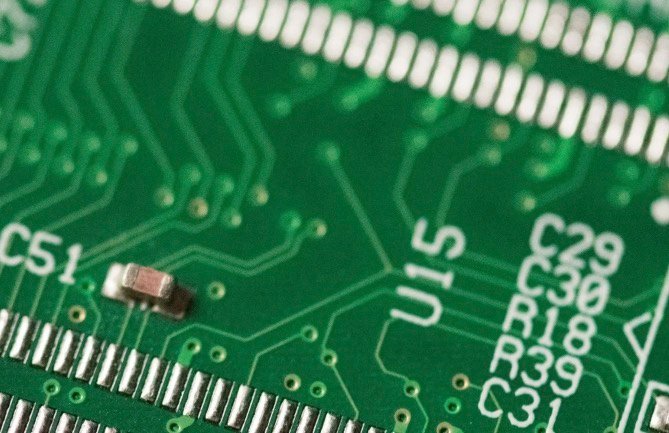
Designing a printed circuit board (PCB) is more accessible than ever, but it’s a skill that requires attention to detail. For beginners, a few common oversights can turn an exciting project into a frustrating experience. Understanding these frequent mistakes is the first step for anyone looking to design and build reliable, functional electronic devices. By learning what to avoid from the start, you can save time, money, and headaches on your PCB design journey.
Choosing the Wrong Software for Your Project
The software you use to design your PCB is your most important tool. The right choice can make the process smooth and efficient, while the wrong one can create unnecessary roadblocks. Your ideal software depends entirely on your project’s complexity and your own experience level.
There is a vast landscape of PCB design software available. You can find everything from free, browser-based tools perfect for beginners to highly advanced professional suites that cost thousands. It’s a common mistake to either jump into a program that is too complex or choose one that lacks the features you will need later on.
Before committing to a software, assess your needs. Are you designing a simple two-layer board for a hobby project or a multi-layer board with high-speed signals for a commercial product? For beginners, a great starting point is a free tool like Gepetto, which runs in your browser and simplifies the process. As you advance, you might look into more powerful options, but always read reviews to see what others in your field are using.
| Software Type | Best For | Example |
|---|---|---|
| Browser-Based / Free | Beginners, Hobbyists, Simple Designs | Gepetto, EasyEDA |
| Open-Source Desktop | Advanced Hobbyists, Professionals | KiCad |
| Professional Suite | Commercial, High-Complexity Designs | Altium Designer, Eagle |
The Critical Importance of Accessible Nodes
No matter how carefully you design your board, you will eventually need to troubleshoot it. Whether you’re checking a voltage, probing a signal, or debugging a communication line, you need physical access to the important connection points, or nodes, on your circuit.
One of the most frustrating moments for any electronics enthusiast is realizing the signal you need to measure is buried under a large component with no accessible test point. Planning for troubleshooting from the beginning is a mark of a good designer. When you are laying out your board, think about which signals are most critical. These include power lines, clock signals, and data buses.
Make it a habit to add small test pads or exposed vias to these key nodes. This simple step takes only a few seconds during the design phase but can save you hours of frustration later. Having these points readily available means you can quickly connect an oscilloscope or multimeter probe without having to do delicate and risky soldering on the pins of an integrated circuit.
Why Component Spacing is Non-Negotiable
A frequent impulse for new designers is to make their PCB as small and compact as possible. While efficiency is a good goal, placing components and traces too close together is a recipe for disaster. Proper spacing is essential for both the electrical and physical integrity of your board.
When electricity flows through the copper traces on your board, they heat up. This causes the copper to expand slightly. If your traces are designed with inadequate clearance, this thermal expansion can cause them to touch, creating a short circuit that can permanently damage your components.
Furthermore, components can interfere with each other electrically. This is known as electromagnetic interference, or EMI. It can cause a wide range of problems that are often difficult to diagnose.
- Analog sensors may give noisy or inaccurate readings.
- High-speed data lines can become corrupted, leading to communication errors.
- Wireless modules like Wi-Fi or Bluetooth can have their range and performance severely degraded.
To avoid this, always follow recommended spacing guidelines and keep sensitive analog components separate from noisy digital or power components.
Maintaining Consistent Component Orientation
The way you orient your components might seem like a minor aesthetic choice, but it has a major impact on assembly and troubleshooting. A board with randomly rotated components is difficult to read and work on. Adopting a consistent orientation standard makes your boards cleaner and much more user-friendly.
The most common convention is to orient all integrated circuits (ICs) in the same direction. Typically, Pin 1 of every IC is placed in the top-left corner. This standard makes it incredibly easy to locate specific pins during testing and debugging. If every component is facing a different way, you have to stop and re-orient yourself for each measurement, which slows down the process and increases the chance of making a mistake.
This consistency is even more important for board assembly. Whether you are soldering the components by hand or using an automated pick-and-place machine, a uniform orientation simplifies the entire process and dramatically reduces the rate of errors.
Forgetting About Design for Manufacturability (DFM)
A design that looks perfect on your computer screen might be impossible or extremely expensive to actually produce. Design for Manufacturability (DFM) is the practice of designing your board while keeping the capabilities and limitations of your manufacturer in mind. Ignoring DFM is a classic beginner mistake that often results in a failed manufacturing run.
Every fabrication house has a specific set of rules for what they can reliably produce. These rules dictate things like the minimum width of a copper trace, the smallest drill size they can use for vias, and the required clearance between different elements on the board.
Before you finalize your design, get the DFM specifications from your chosen manufacturer and run a check in your design software. This ensures that your design is not only functional but also manufacturable at a reasonable cost. Failing to do this can lead to your order being rejected or, worse, receiving a batch of non-functional boards.
Frequently Asked Questions about PCB Design Mistakes
What is the most common mistake for PCB beginners?
The most frequent mistake is improper spacing. Beginners often try to pack components too tightly, which can lead to short circuits from thermal expansion and performance issues due to electromagnetic interference.
How much space should I leave between copper traces?
This depends on the voltage and the manufacturer’s capabilities. A good general rule for low-voltage signals is to use a minimum clearance of 6-10 mils (0.15-0.25mm), but always check your manufacturer’s specific DFM guidelines for a reliable number.
Is free PCB design software good enough for hobby projects?
Absolutely. Modern free and open-source software like KiCad and EasyEDA are incredibly powerful and more than capable of handling complex hobbyist projects. They are a great way to learn without a financial investment.
What is electromagnetic interference (EMI) in a PCB?
EMI is unwanted electrical noise generated by one component that negatively affects the performance of another. For example, a high-speed processor could create interference that disrupts the sensitive readings of an analog sensor on the same board.
Why is component orientation so important?
A consistent component orientation, such as having Pin 1 in the same corner for all chips, makes the board much easier to assemble, test, and debug. It reduces the chance of errors during soldering and saves time during troubleshooting.


Leave a Comment